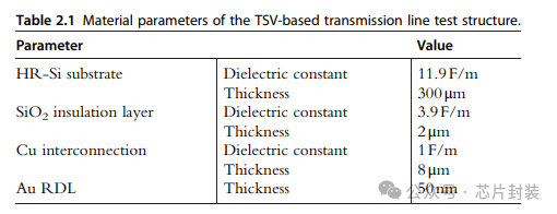
The resistivity of the Si substrate is one of the significant factors related to the HF insertion loss of TSVs. In this experiment, HR-Si wafers with resistivity greater than 2 kΩcm were used. Design of a coaxial ladder TSV structure consisting of different-sized hollow vias was employed (Fig. 2.5). During the fabrication process, thermal oxidization was performed to produce SiO2 as the insulation between TSV metal and the Si substrate. The vias were metallized by conformal Cu electroplating for the transmission of electrica signals. There was also a Ti/Cu barrier/adhesion layer between the plated Cu and SiO2, which avoids the diffusion of Cu into the substrate and increases the adhesion of the Cu with the oxide [4]. Cu was used to establish the electrical connection in a rewiring layer on the surface. Electroless nickel electroless palladium immersion gold (ENEPIG) was used for the bonding pads in order to fit the RF/MW microelectronics integrated devices, while Au contacts are widely used in these chips made of group III-V semiconductor materials. The material parameters are summarized in Table 2.1.
Si衬底的电阻率是影响tsv高频插入损耗的重要因素之一。本实验采用电阻率大于2 kΩcm的HR-Si晶片。采用不同尺寸空心通孔组成的同轴梯式TSV结构设计(图2.5)。在制作过程中,通过热氧化生成SiO2作为TSV金属与Si衬底之间的绝缘层。通过共形镀铜对通孔进行金属化处理,用于传输电信号。镀Cu与SiO2之间还存在Ti/Cu屏障/粘附层,避免了Cu向基体扩散,增加了Cu与氧化物的附着力[4]。铜用于在表面的重新布线层中建立电气连接。为了适应RF/MW微电子集成器件,焊盘采用了化学镍-化学钯浸金(ENEPIG),而这些III-V族半导体材料制成的芯片则广泛采用金触点。材料参数汇总如表2.1所示。
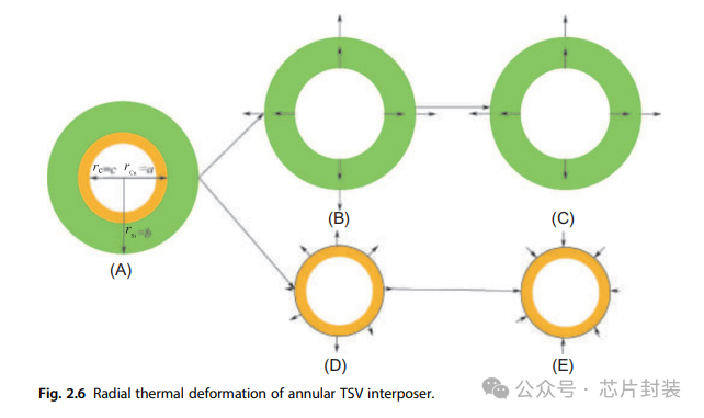
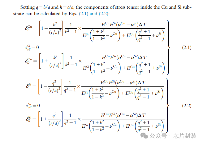
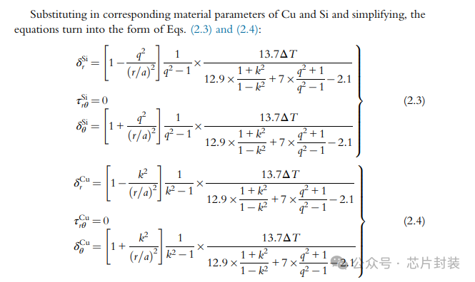
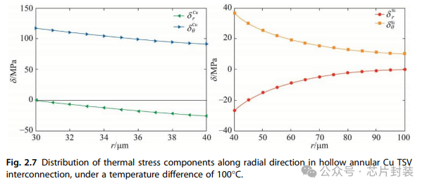
Assuming the outer radius of the Si substrate is 120μm and the inner and outer radii of the Cu tube are 36μm and 40μm, respectively, and a temperature difference of 100°C is loaded, the distribution of stress components along the radial direction are calculated and shown in Fig. 2.7. As shown, the maximum stress occurs at the common boundary of Cu and Si. As for the Cu, the changing of both radial and annular stress are steady and nearly linear. As for the Si substrate, inside 60μm, both radial and annular stress change dramatically, while outside 60μm, both of them change less significantly and tend to be stable. Fig. 2.8 shows the change of stress at the common boundary with q. It can be假设Si衬底的外半径为120μm, Cu管的内外半径分别为36μm和40μm,加载温差为100℃,计算应力分量沿径向的分布,如图2.7所示。如图所示,最大应力出现在Cu和Si的共同边界处。Cu的径向应力和环向应力的变化均稳定且接近线性。对于Si衬底,60μm内径向应力和环向应力变化较大,60μm外径向应力和环向应力变化较小,趋于稳定。图2.8为共边界处应力随q的变化情况
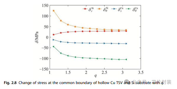
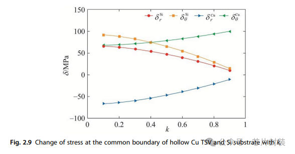
found that the stress components tend to be stable when the outer radius of the Si substrate reaches twice the outer radius of hollow Cu TSV. In this scenario, adjacent TSVs should be spaced by twice their outer radius to reduce or avoid the coupling of thermal stress. As shown in Fig. 2.9, the value of each of the thermal stress components increases as k decreases. As the Cu sidewall gets thicker, the thermal stress in the radial direction becomes greater; in other words, hollow annular Cu TSV should have higher thermal mechanical reliability than filled Cu TSV at a given condition. The optimization can be determined by using a 3D model. Considering the effects in the depth direction, by insulation layers, and so on, build up a 3D model and perform FEA. Fig. 2.10 shows the thermal stress distribution cloud graph of cylindrical TSV and ladder TSV under a 1K temperature difference. It can be seen that the发现当Si衬底外半径达到空心Cu TSV外半径的2倍时,应力分量趋于稳定。在这种情况下,相邻的tsv间距应为其外半径的两倍,以减少或避免热应力的耦合。如图2.9所示,各热应力分量的值随着k的减小而增大。随着铜侧壁厚度的增加,径向热应力增大;也就是说,在一定条件下,空心环形铜TSV应具有比填充型铜TSV更高的热机械可靠性。优化可以通过使用三维模型来确定。考虑了深度方向、保温层等方面的影响,建立了三维模型并进行了有限元分析。图2.10为温差为1K时圆柱形TSV和梯形TSV的热应力分布云图。可以看出,
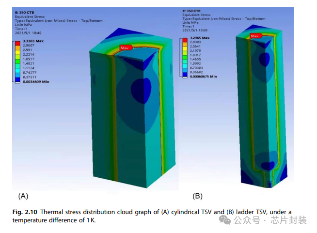
maximum stress in the ladder structure is smaller than that in the cylindrical structure. That implies that the design here is not only beneficial to process, but also performs better in term of thermal mechanical reliability
梯状结构的最大应力小于圆柱结构。这表明,这种设计不仅有利于工艺,而且在热机械可靠性方面也有较好的表现
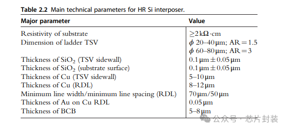
Based on the discussed ladder structure TSV, a process for the RF HR-Si interposer is designed (Fig. 2.11). The main technical parameters are summarized in Table 2.2. The general process flow of fabrication is as follows:
基于所讨论的阶梯结构TSV,设计了RF HR-Si中间体的工艺(图2.11)。主要技术参数如表2.2所示。制造的一般工艺流程如下:
(1) An Si wafer of 300μm, which is double-sided polished and about 3 kΩcm in resistivity, is provided.
(2) Etch from both sides to open through vias. Perform DRIE from one and then the other side after photolithography to yield ladder structure TSVs. The large vias should be 80μm in diameter and 240μm in depth, while the small vias should be 40μm in diameter and 60μm in depth.
(3) Perform RCA standard cleaning to remove any impurity residual, which may contaminate the HR-Si substrate in the following high-temperature process and increase the insertion loss.
(4) Establish high-quality insulation layer. By performing high-temperature thermal oxidation, forming a layer of 100-nm firm SiO2 on the surface of the substrate as well as the sidewall of vias.
(1)提供了一块300μm的双面抛光硅晶片,其电阻率约为3 kΩcm。
(2)从两侧蚀刻开通孔。光刻后从一侧进行drive,然后从另一侧进行drive,得到阶梯结构的tsv。大孔直径为80μm,深度为240μm,小孔直径为40μm,深度为60μm。
(3)进行RCA标准清洗,去除任何杂质残留,这些杂质可能会在接下来的高温过程中污染HR-Si衬底,增加插入损耗。
(4)建立优质保温层。通过高温热氧化,在衬底表面和通孔侧壁上形成一层100 nm坚固的SiO2。
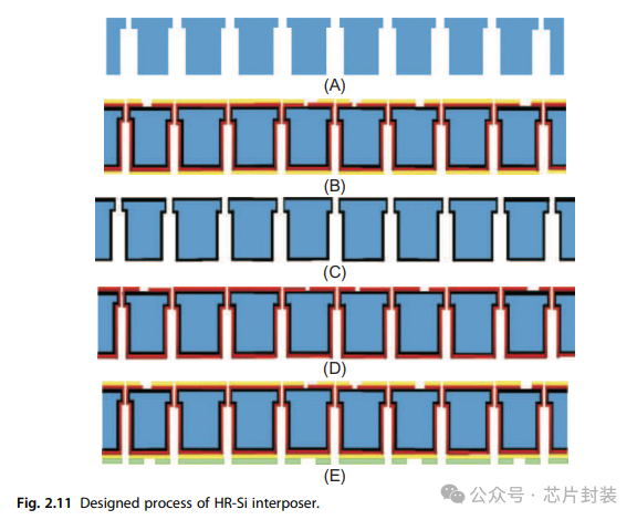
(5) Perform TSV metallization and the establishment of surface rewiring layer. Sputter 200 nm of Ti as adhesion layer and 2μm of Cu as seed layer onto both sides. Perform photolithography to produce patterned masks. Perform plasma cleaning to remove residue and activate the Cu seed layer. Electroplate 8–10μm of Cu
(5)进行TSV金属化,建立表面重布线层。在两侧溅射200 nm的Ti作为附着层,2μm的Cu作为种子层。使用光刻技术制作有图案的面具。进行等离子清洗以去除残留物并激活铜种子层。电镀8-10μm的Cu
by controlling the time of performing, concentration of electroplate liquid, current density, etc.Cu TSVs and RDL rewiring lines are formed. Then remove the masks and wet-etch to remove the Cu seed layer and then the Ti adhesion layer.
(6) Plate Ni and Au. Perform electroless Ni plating and Au electroless plating to deposit 3μm of Ni and 50 nm of Au onto the surface Cu layers on both sides simultaneously.
(7) Passivation. A layer of BCB or dry photosensitive film is coated and patterned on the side of large vias for further bumping.
(8) Screen, dice, and single out.
通过控制执行时间、电镀液浓度、电流密度等,形成cu tsv和RDL重接线。然后去除掩模,湿蚀去除Cu种子层,再去除Ti附着层。
(6)镀镍和镀金。化学镀Ni和化学镀Au,同时在两侧的Cu层表面沉积3μm的Ni和50 nm的Au。
(7)钝化。在大孔的侧面涂上一层bbcb或干感光膜,以便进一步碰撞。
(8)筛,分,挑。
